What is Scanning Electron Microscopy (SEM)

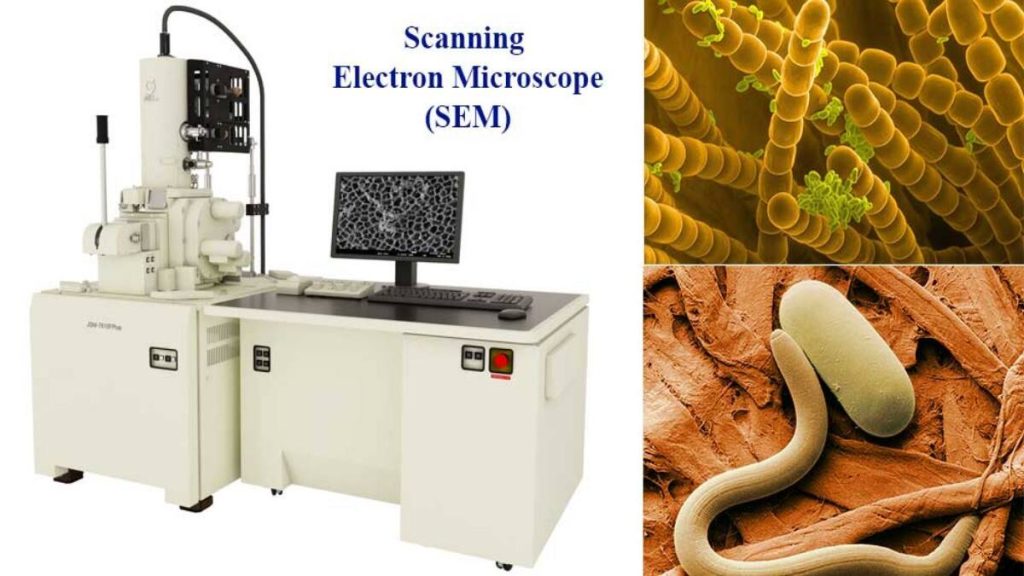
A typical SEM instrument, showing the electron column, sample chamber, EDS detector, electronics console, and visual display monitors.
The scanning electron microscope (SEM) uses a focused beam of high-energy electrons to generate a variety of signals at the surface of solid specimens. The signals that derive from electron-sample interactions reveal information about the sample including external morphology (texture), chemical composition, and crystalline structure and orientation of materials making up the sample. In most applications, data are collected over a selected area of the surface of the sample, and a 2-dimensional image is generated that displays spatial variations in these properties. Areas ranging from approximately 1 cm to 5 microns in width can be imaged in a scanning mode using conventional SEM techniques (magnification ranging from 20X to approximately 30,000X, spatial resolution of 50 to 100 nm). The SEM is also capable of performing analyses of selected point locations on the sample; this approach is especially useful in qualitatively or semi-quantitatively determining chemical compositions (using EDS), crystalline structure, and crystal orientations (using EBSD). The design and function of the SEM is very similar to the EPMA and considerable overlap in capabilities exists between the two instruments.
Fundamental Principles of Scanning Electron Microscopy (SEM)
Accelerated electrons in an SEM carry significant amounts of kinetic energy, and this energy is dissipated as a variety of signals produced by electron-sample interactions when the incident electrons are decelerated in the solid sample. These signals include secondary electrons (that produce SEM images), backscattered electrons (BSE), diffracted backscattered electrons (EBSD that are used to determine crystal structures and orientations of minerals), photons (characteristic X-rays that are used for elemental analysis and continuum X-rays), visible light (cathodoluminescence–CL), and heat. Secondary electrons and backscattered electrons are commonly used for imaging samples: secondary electrons are most valuable for showing morphology and topography on samples and backscattered electrons are most valuable for illustrating contrasts in composition in multiphase samples (i.e. for rapid phase discrimination). X-ray generation is produced by inelastic collisions of the incident electrons with electrons in discrete ortitals (shells) of atoms in the sample. As the excited electrons return to lower energy states, they yield X-rays that are of a fixed wavelength (that is related to the difference in energy levels of electrons in different shells for a given element). Thus, characteristic X-rays are produced for each element in a mineral that is “excited” by the electron beam. SEM analysis is considered to be “non-destructive”; that is, x-rays generated by electron interactions do not lead to volume loss of the sample, so it is possible to analyze the same materials repeatedly.
Scanning Electron Microscopy (SEM) Instrumentation – How Does It Work?

Essential components of all SEMs include the following:
· Electron Source (“Gun”)
· Electron Lenses
· Sample Stage
· Detectors for all signals of interest
· Display / Data output devices
· Infrastructure Requirements:
o Power Supply
o Vacuum System
o Cooling system
o Vibration-free floor
o Room free of ambient magnetic and electric fields
SEMs always have at least one detector (usually a secondary electron detector), and most have additional detectors. The specific capabilities of a particular instrument are critically dependent on which detectors it accommodates.
Applications

The SEM is routinely used to generate high-resolution images of shapes of objects (SEI) and to show spatial variations in chemical compositions: 1) acquiring elemental maps or spot chemical analyses using EDS, 2)discrimination of phases based on mean atomic number (commonly related to relative density) using BSE, and 3) compositional maps based on differences in trace element “activitors” (typically transition metal and Rare Earth elements) using CL. The SEM is also widely used to identify phases based on qualitative chemical analysis and/or crystalline structure. Precise measurement of very small features and objects down to 50 nm in size is also accomplished using the SEM. Backescattered electron images (BSE) can be used for rapid discrimination of phases in multiphase samples. SEMs equipped with diffracted backscattered electron detectors (EBSD) can be used to examine microfabric and crystallographic orientation in many materials.
Strengths and Limitations of Scanning Electron Microscopy (SEM)?
Strengths
There is arguably no other instrument with the breadth of applications in the study of solid materials that compares with the SEM. The SEM is critical in all fields that require characterization of solid materials. While this contribution is most concerned with geological applications, it is important to note that these applications are a very small subset of the scientific and industrial applications that exist for this instrumentation. Most SEM’s are comparatively easy to operate, with user-friendly “intuitive” interfaces. Many applications require minimal sample preparation. For many applications, data acquisition is rapid (less than 5 minutes/image for SEI, BSE, spot EDS analyses.) Modern SEMs generate data in digital formats, which are highly portable.
Limitations
Samples must be solid and they must fit into the microscope chamber. Maximum size in horizontal dimensions is usually on the order of 10 cm, vertical dimensions are generally much more limited and rarely exceed 40 mm. For most instruments samples must be stable in a vacuum on the order of 10-5 – 10-6 torr. Samples likely to outgas at low pressures (rocks saturated with hydrocarbons, “wet” samples such as coal, organic materials or swelling clays, and samples likely to decrepitate at low pressure) are unsuitable for examination in conventional SEM’s. However, “low vacuum” and “environmental” SEMs also exist, and many of these types of samples can be successfully examined in these specialized instruments. EDS detectors on SEM’s cannot detect very light elements (H, He, and Li), and many instruments cannot detect elements with atomic numbers less than 11 (Na). Most SEMs use a solid state x-ray detector (EDS), and while these detectors are very fast and easy to utilize, they have relatively poor energy resolution and sensitivity to elements present in low abundances when compared to wavelength dispersive x-ray detectors (WDS) on most electron probe microanalyzers (EPMA). An electrically conductive coating must be applied to electrically insulating samples for study in conventional SEM’s, unless the instrument is capable of operation in a low vacuum mode.


