Electron microscopes have emerged as a powerful tool for the characterization of a wide range of materials. Their versatility and extremely high spatial resolution render them a very valuable tool for many applications. The two main types of electron microscopes are the Transmission Electron Microscope (TEM) and the Scanning Electron Microscope (SEM). In this blog we briefly describe their similarities and differences.
The difference between SEM and TEM
The main difference between SEM and TEM is that SEM creates an image by detecting reflected or knocked-off electrons while TEM uses transmitted electrons (electrons which are passing through the sample) to create an image. As a result, TEM offers valuable information on the inner structure of the sample, such as crystal structure, morphology and stress state information, while SEM provides information on the sample’s surface and its composition.
Working Principle of Scanning Electron Microscopes and Transmission Electron Microscopes
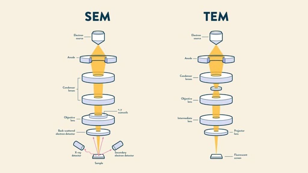
Let’s start with the similarities. For both techniques, electrons are used in order to acquire images of samples. Their main components are the same;
- An electron source;
- A series of electromagnetic and electrostatic lenses to control the shape and trajectory of the electron beam;
- Electron apertures.
All of these components live inside a chamber which is under high vacuum. Now over to the differences. SEMs use a specific set of coils to scan the beam in a raster-like pattern and collect the scattered electrons (read more about the different type of electrons detected in a SEM). The transmission electron microscopy (TEM) principle, as the name suggests, is to use the transmitted electrons; the electrons which are passing through the sample before they are collected. As a result, TEM offers invaluable information on the inner structure of the sample, such as crystal structure, morphology and stress state information, while SEM provides information on the sample’s surface and its composition.
Moreover, one of the most pronounced differences between the two methods is the optimal spatial resolution that they can achieve; SEM resolution is limited to ~0.5 nm, while with the recent development in aberration-corrected TEMs, images with spatial resolution of even less than 50 pm have been reported.
Which electron microscopy technique is best for your analysis?
This all depends on what type of analysis you want to perform. For example, if you want to get information on the surface of your sample, like roughness or contamination detection, then you should choose a SEM. On the other hand, if you would like to know what the crystal structure of your sample is, or if you want to look for possible structural defects or impurities, then using a TEM is the only way to do so. SEMs provide a 3D image of the surface of the sample whereas TEM images are 2D projections of the sample, which in some cases makes the interpretation of the results more difficult for the operator. Due to the requirement for transmitted electrons, TEM samples must be very thin, generally below 150 nm, and in cases that high-resolution imaging is required, even below 30 nm, whereas for SEM imaging there is no such specific requirement.
This reveals one more major difference between the two techniques; sample preparation. SEM samples require little or no effort for sample preparation and can be directly imaged by mounting them on an aluminum stub. In contrast, TEM sample preparation is a quite complex and tedious procedure that only trained and experienced users can follow successfully. The samples need to be very thin, as flat as possible, and the preparation technique should not induce any artefacts (such as precipitates or amorphization) to the sample. Many methods have been developed, including electropolishing, mechanical polishing and focused ion beam milling. Dedicated grids and holders are used to mount the TEM samples.
SEM vs TEM: differences in operation
The two EM systems also differ in the way they are operated. SEMs usually use acceleration voltages up to 30 kV, while TEM users can set it in the range of 60 – 300kV. The magnifications that TEMs offer are also much higher compared to SEMs: TEM users can magnify their samples by more than 50 million times, while for the SEM this is limited up to 1-2 million times.
However, the maximum Field of View (FOV) that SEMs can achieve is far larger than TEMs, which users can only use to image a very small part of their sample. Similarly, the depth of field of SEM systems are much higher than in TEM systems.
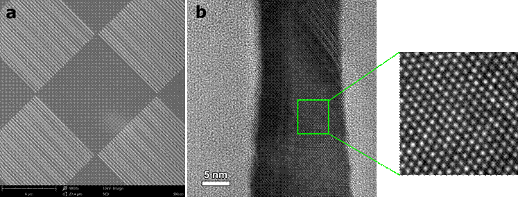
Figure 1: Electron microscopy images of silicon. a) SEM image with SED offers information on the morphology of the surface, while b) TEM image reveals structural information about the inner sample.
In addition, the way images are created are different in the two systems. In SEMs, samples are positioned at the bottom of the electron column and the scattered electrons (back-scattered or secondary) are captured by electron detectors. Photomultipliers are then used to convert this signal into a voltage signal, which is amplified and gives rise to the image on a PC screen.
In a TEM microscope, the sample is located in the middle of the column. The transmitted electrons pass through it, and through a series of lenses below the sample (intermediate and projector lenses). An image is directly shown on a fluorescent screen or via a charge-coupled device (CCD) camera, onto a PC screen.
| SEMTEMType of electronsScattered, scanning electronsTransmitted electronsHigh tension~1 – 30 kV~60 – 300 kVSpecimen thicknessAnyTypically <150 nmType of info3D image of surface2D projection image of inner structureMax. magnificationUp to ~1 – 2 million timesMore than 50 million timesMax. FOVLargeLimitedOptimal spatial resolution~0.5 nm< 50 pmImage formationElectrons are captured and counted by detectors, image on PC screenDirect imaging on fluorescent screen or PC screen with CCDOperationLittle or no sample preparation, easy to useLaborious sample preparation, trained users required |
Table I: Summary of the main differences between a SEM and a TEM
Generally, TEMs are more complex to operate. TEM users require intensive training before being able to operate them. Special procedures need to be performed before every use, with several steps included that ensure that the electron beam is perfectly aligned. In Table I, you can see a summary of the main differences between a SEM and a TEM.
Combining SEM and TEM technology
There is one more electron microscopy technique to mention, which is a combination of TEM and SEM, namely Scanning Transmission Electron Microscopy (STEM). It can be applied to both systems, but its full capabilities are revealed when applied to a TEM tool. Most modern TEMs can be switched to “STEM mode” and the user only needs to alter their alignment procedure. In STEM mode, the beam is finely focused and scans the sample area (as SEM does), while the image is generated by the transmitted electrons (like in TEM).
When working in STEM mode the users can take advantage of the capabilities of both techniques; they can look at the inner structure of samples with very high resolving power (even higher than TEM resolution), but also use other signals like X-rays and electron energy loss. These signals can be used in spectroscopic techniques; the energy-dispersive X-ray spectroscopy (EDX) and electron energy loss spectroscopy (EELS). Of course, EDX is also a common practice in SEM systems and is used to identify the chemical composition of samples by detecting the characteristic X-rays that are emitted from the materials when they are bombarded with electrons. EELS can only be realized in a TEM system working in STEM mode and enables the investigation of the atomic and chemical composition, the electronic properties as well as local thickness measurements of materials.
Choosing between SEM and TEM
From everything we have mentioned, it is clear that there is no “better” technique; it all depends on the type of analysis that you require. TEM is the choice when you want to get information from the inner structure, while SEM is preferred when surface information is required. Of course, major decision factors are the big price difference between the two systems, as well as the ease of use. TEMs may enable much more resolving power and versatility to the user, but they are much more expensive and larger than SEMs and require more effort in order to acquire and interpret results. To discover more about SEM and see if it fits your research requirements, you can take a look at our free e-guide: How to choose a Scanning Electron Microscope. This E-guide is intended to assist you in choosing the most suitable Scanning Electron Microscope (SEM) systems for your research.